SBOA531 November 2021 INA901-SP
Design Goals
| Input | Output | Supply | Common-Mode Voltage | Error | Total Ionizing Dose | Single Event Immunity | ||
|---|---|---|---|---|---|---|---|---|
| ILOAD, MIN | ILOAD, MAX | VOUT, min | VOUT, max | VS | VCM | Output Error | TID | SEL |
| –7.5 A | 7.5 A | 500 mV | 3.5 V | 5 V | 0 V | < 2% | 50 krad (Si) | 75 MeV × cm2 /mg |
Design Description
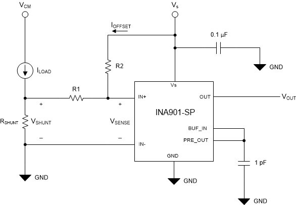
This circuit utilizes passive components (R1 and R2 in the following schematic) to produce a referred to input (RTI) offset that biases the sense input, and achieves bidirectional sensing from a unidirectional current sense amplifier, the INA901-SP. In this design, the normal operating load is from –7.5 A to 7.5 A, with a supply voltage of 5 V. This topology may be used for other supply voltages, but the equations corresponding to offset generation will change accordingly. In addition to this functionality, this circuit implements the INA901-SP, which is a Radiation-Hardness-Assured (RHA), 50-krad (Si) capable device at Low Dose Rate, that is also Single Event Latch-up (SEL) Immune to 75 MeV-cm2/mg at 125°C. The solution presented in this circuit is a low-side implementation, with a common-mode voltage of approximately 0 V.
Design Notes
- This topology is meant for low side implementation, where the IN– pin of the INA901-SP is referenced to GND. While other implementations may be successful, this design is unable to be implemented where VCM > Vs, as the current must flow toward the IN+ pin to achieve the necessary offset. Therefore, the common-mode voltage of the IN+ pin must be less than that of the supply voltage to ensure valid operation.
- The offset current created by the design process shows that, as a consequence, the offset voltage point deviates slightly with the sense voltage, producing a linear error along with the sense voltage.
- Because this is a low-side implementation, the trade-offs that come with measuring on the low side are in effect here. This includes the inability of the load to detect ground faults.
- When designing with the INA901-SP, be careful to ensure the full-scale input range of the device remains above 20 mV for best performance. If VSENSE is allowed below 20 mV, the device may produce additional errors inside of this operating condition. See the INA901-SP Radiation Hardened, –15-V to 65-V Common Mode, Unidirectional Current-Shunt Monitor data sheet for more information.
- While this circuit provides the ability to measure in multiple directions, it does not change the fact that the INA901-SP is inherently a unidirectional device. This infers that one direction of current sensing will be more accurate than the other, as one direction will measure towards the offset voltage of the device, leading to increased error in this direction. The effects of this may be mitigated in part by the use of a one-point calibration, and is discussed later in this document.
Design Steps
- Design the Offset Current:
The offset current will ultimately flow over R1 to create the RTI offset sense
voltage, but is determined by the supply voltage and R2. Here, errors will be
present due to:
- The input bias current of the IN+ pin will pull a few mA of current from the ideal calculation and this results in a negligible amount of error
- As shown in the design equation, the voltage present on the IN+ pin with respect to GND will also have bearing. It can be inferred (and confirmed in simulation) that this will result in a small linear error over the full-scale range as the generated shunt voltage moves this voltage on the IN+ pin. Here, we approximate this voltage as approximately equal to 0 V.
The offset current with this approximation is given by:
- Choose RSHUNT to Optimize Input Range: With the RTI offset designed, a shunt may now be chosen for the desired sensing range. For the INA901-SP, maintain the lower sensing bound to > 20 mV for optimal performance. This shows that the amount of sensing headroom from VREF is:
From the desired –7.5 A design target, it is calculated that the maximum allowable shunt to achieve this goal is:
As the ILOAD design target in the remaining direction is symmetric about VREF, 10 mΩ is selected to complete the design. The final input VSENSE swing is calculated with the following:
The expected corresponding output is as follows:
- Verify Shunt Derating is Sufficient: A necessary aspect of proper shunt design is ensuring that the design choice has sufficient margin for power derating. As the device heats in the environment, the amount of power the shunt is capable of dissipating is derated by a certain factor. For continuous sensing, this factor can be as high as 0.6. Taking this into account, for the design, a shunt must be chosen that is rated for at least the following:
So for a successful design, a shunt of at least 1-W rated power is chosen for continuous sensing.
- Examine Error. Calibrate if Necessary: As discussed in previous sections, it is expected that the current-sense amplifier will be more accurate in the direction of measurement as the output is driven toward supply. Less accurate measurements are expected as the sense voltage decreases, and errors from the offset voltage begin to dominate the measurement. A potential solution for this is to perform at least a one-point calibration in logic to reduce the effects of the offset voltage.
A one-point calibration is performed by applying the condition, to the system, capturing the actual value output by the INA901-SP, and maintaining the difference between this value and the calculated ideal in memory. The output of the device is then consistently shifted by this amount. An example of the effects of this are shown in the following simulated results.
Design Simulations
DC Sweep Results, –7.5 A < ILOAD < 7.5 A
 INA901-SP Low-Side Bidirectional Circuit Performance Over Load
 Error Curves, Pre- and Post-Calibration From Simulation Data
Simulated results show that, as expected, there is a slight change to the offset current as the voltage of IN+ shifts with VSHUNT. Calibration of the raw data results in a full-scale error of < 1%, thus meeting the design goal. It should be noted that parameters such as device offset and input bias currents in TINA-TI models reflect typical data sheet parameters, and additional error may be exhibited pre- and post-calibration due to variation in these parameters. For additional information on one-point calibration and examples involving real bench tested data, see the Bidirectional Topologies for the INA901-SP.
Design References
See the TI Precision Labs, Current Sense Amplifiers video series.
| INA901-SP | |
|---|---|
| VS | 2.7 V to 16 V |
| VCM | –15 V to 65 V |
| VOUT | GND+3 mV to VS – 50 mV, typical |
| VOS | ±500 μV, typical |
| Iq | 350 μA, typical |
| IB | ±8 μA, typical |
TID Characterization (ELDRS-Free) |
50 krad (Si) |
SEL Immune to LET |
75 MeV-cm2/mg |
| INA901-SP | |